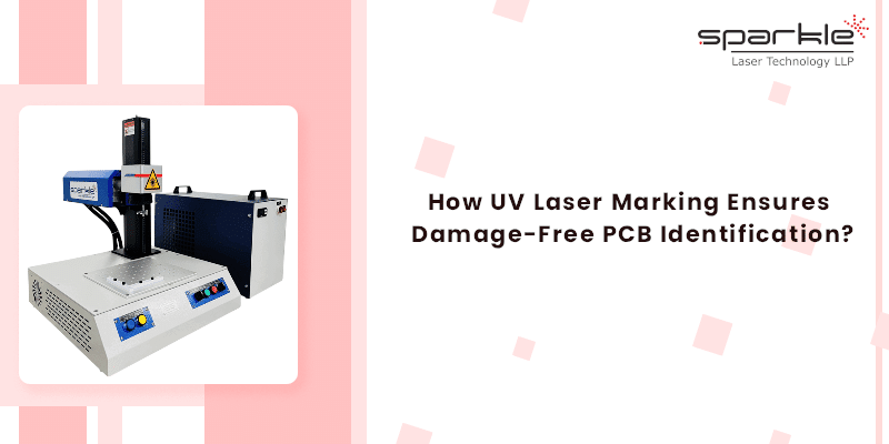
Printed circuit boards, or PCBs, are the backbone of modern electronics. From smartphones and laptops to medical devices and industrial controllers, almost every electronic device depends on them. But when PCBs are this small, complex, and sensitive, even something as simple as marking an ID number can become a challenge.
That’s where UV laser marking steps in!
Traditional marking methods are capable of scratching surfaces, overheating components, or fading with time. UV laser marking is a more hygienic and safer method of marking which does not entail any risk to the structure or the performance of the PCBs. How this device operates and the factors that make it the most reliable option for nondestructive PCB identification are topics that we will delve into!
Why PCB Identification Matters More Than Ever?
PCB identification goes beyond merely putting a serial number or logo. It mainly includes:
- Traceability during manufacturing
- Quality control and inspection
- Warranty tracking
- Repair and replacement processes
- Regulatory compliance
The trend is towards smaller and more powerful electronics and less room for error. Inadequately marked PCBs may cause difficulties during scanning, wrong identification, or even the failure of the device. Thus, manufacturers have to equip themselves with marking solutions that deliver accuracy, permanence, and are non-destructive.
Challenges with Traditional PCB Marking Methods
Before UV laser marking became popular, PCBs were often marked using methods like ink printing, labels, or mechanical engraving. While these approaches worked to some extent, they came with limitations.
Any ink-based markings on the board may have their inks smeared, faded, or worn off during soldering or cleaning. In addition, labels may detach gradually or cause components to become electrically insulated. On the other hand, mechanical engraving exposes the PCB to scratching of copper traces and damages the board surface.
Printed circuit boards also have materials that are sensitive to heat. Overheating can result in the weakening of solder joints, warping of substrates, or even the cooling of the adjacent components. So, it is obvious that a better way had to be found.
What Makes UV Laser Marking Different?
UV laser marking employs ultraviolet light to generate marks via a photochemical reaction, rather than a thermal one. This is the main factor why it is highly compatible with PCBs.
UV lasers have a shorter wavelength as compared to infrared or fiber lasers. Hence, they can mark ultra-fine details with very little heat being generated. The material is not combusted or melted; the surface is simply interacted with at a molecular level.
In simple terms, UV laser marking “etches” information onto the PCB without stressing it. Modern UV laser marking machines use ultraviolet light to create damage-free and permanent identification on PCBs without harming components.
Damage-Free Marking for Sensitive PCB Materials
PCBs consist of layers of different materials, such as fiberglass, resins, copper tracks, and protective coatings. UV laser marking is a method that takes into account this nature of the material.
As the heat impact is very small:
- Copper traces are not affected.
- Solder masks do not crack or peel.
- Board flatness is kept.
- Close components do not get heated.
Thus, UV laser marking is a perfect solution to be used both for bare boards and assembled PCBs, even those with densely packed layouts.
High Precision for Small and Complex Designs
Modern PCBs don’t leave much room for markings. Sometimes, the available space is just a few millimetres wide. UV laser marking excels here.
It can produce:
- Crisp serial numbers
- Tiny alphanumeric codes
- High-resolution QR codes
- Barcodes readable by automated scanners
Even at micro sizes, the marks remain sharp and consistent. This precision is especially valuable for industries like consumer electronics, medical equipment, and aerospace, where space is limited and accuracy is critical. For extremely fine and accurate coding needed on circuit boards, a high-precision UV laser marking machine delivers crisp alphanumeric codes and traceable identifiers.
Permanent Identification That Lasts
UV laser marking is durable to one extreme. The point, basically, is that it is simply the material itself that is altered by the laser, not a new layer inked on or whatsoever. Hence, unlike ink or stickers, UV laser markings cannot be faded by time, heat or chemical exposure. They can withstand a soldering process, a washing cycle, or simply long usage.
Such longevity guarantees that the PCB identifications are going to be still visible well beyond the product’s life span, from the manufacturing stage up to the end-of-life servicing one.
Supporting Traceability and Quality Control
Traceability plays a major role in the production of electronics. Most of the time, each PCB has to be traced all the way from its manufacturing to its final assembly.
One way to achieve that is with the use of UV laser marking which makes the identification visually clear and consistent. Any code that can be scanned can be used to associate each board with its batch, production date, or inspection history.
In case a defect is discovered at a later time, producers can very fast locate its origin, thus, they are able to lessen the costs of recalls and enhance the level of their own accountability. Such a degree of managing power is almost impossible if one relies on the markings that get faded or damaged.
Clean and Contamination-Free Process
Manufacturers often choose UV laser engraving and marking options because they avoid inks, solvents, and consumables that could contaminate sensitive electronics.
That means:
- No chemical residue on PCBs
- No risk of contamination
- No ongoing material costs
For industries that demand cleanroom-friendly processes, such as medical electronics or semiconductor manufacturing, this is a huge advantage.
Easy Integration into PCB Production Lines
UV laser marking setups are built to function effortlessly with automated surroundings. Hence, they can be incorporated into printed circuit board (PCB) assembly lines without causing a production hold.
In fact, the whole operation is very quick and can be done numerous times in the same way once the device is set up. There is no necessity for the workers to frequently change the settings since the output remains stable for different large volumes of products.
Such dependability is instrumental in ensuring that the production process does not lose its pace, and at the same time, the marking gets better in quality.
Real-World Applications of UV Laser Marking on PCBs
UV laser marking is widely used across different stages of PCB manufacturing.
Bare PCB Marking
Before assembly, these are typically used for adding board IDs, manufacturer details, or lot numbers.
Assembled PCB Identification
Enables marking of the accomplished boards in a non, visual way without the destruction of the soldered components.
Very Compact Boards
Perfect for marking extremely small PCBs that are used in smartphones, wearables, and IoT devices.
Regulated Industries
Facilitates medical, automotive, and aerospace electronics where traceability is required, thus, traceability is mandatory.
Cost Benefits Over Time
In most cases, UV laser systems need an upfront investment, but over time, they tend to cut down the overall costs.
Producers save money on consumables, minimise the rework that is caused by the errors in the marking, and decrease the rejection rate. Higher overall productivity is the result of less downtime and fewer defects.
When the return on investment is combined with the product’s long service life and reliability, it becomes very obvious.
Why UV Laser Marking Fits the Future of Electronics?
The trend of electronics is to become smaller, smarter, and more complicated. The methods of PCB identification have to be at the same level without increasing the risk.
UV laser marking is a perfect match for this coming future. It has all the advantages of precision without causing any damage, permanence without any pollution, and efficiency without any compromise.
As the manufacturers will be continuously pushing the limits, the technologies that will support both the quality and the performance will become mandatory, not a choice.
Final Thoughts
PCB identification may seem like a small step in the manufacturing process, but it has a big impact on quality, traceability, and reliability. UV laser marking offers a modern solution that respects the delicate nature of PCBs while delivering clear, permanent results.
By eliminating heat damage, surface stress, and fading issues, it ensures that every board carries its identity safely and accurately. For manufacturers focused on precision and long-term performance, UV laser marking is proving to be the smarter way forward.
FAQs
1. Why is UV laser marking considered safe for PCB identification?
UV laser marking generates very minimal heat and essentially uses a photochemical process instead of a thermal one. As a result, it does not harm the parts of the PCB that are made of sensitive materials; copper can be traced, and even components that are close to the area, thus making it a safe choice for both bare and assembled boards.
2. Can UV Laser Marking Be Used on Fully Assembled PCBs?
Sure! UV laser marking is accurate and light enough to be done on a fully assembled PCB without any solder joints, surface coatings, or electronic components being affected. So, it is feasible for identification even at the later stages of production.
3. How Long Are UV Laser Markings on PCBs?
UV laser marks are permanent, and they are resistant to heat, cleaning chemicals, and normal friction. The markings stay readable throughout the whole life cycle of the PCB, starting from manufacturing and testing and going to long-term use and servicing.